Week01
Universal Turing Machine
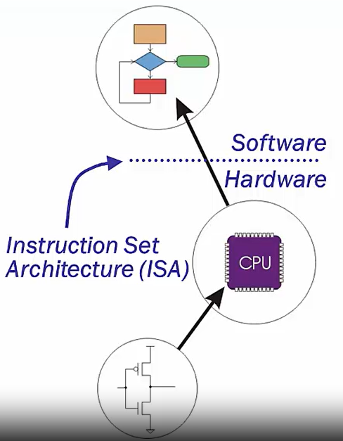
A programmable computer is effectively a Universal Turing Machine (minus infinite memory)
A “program” describes a computation
One that can “simulate” any other Turing machine by in putting a description of that machine’s behavior rules
The behavior is no longer “hard-coded”!
In theory, a computer can compute anything that’s possible to compute…
- Given enough memory and time
Technology
Moore’s law
Predicted doubling of capacity every 24 months -> Cost halves every two years.
Has generally held true
Processor
Executes applicationsthat have been brokendown into sequencesof simple instructions
Use digital logic circuits, made up of transistors
Abstraction
hardware/software
ISA is the boundary
hardware: ISA, Microarchitecture,Logic Circuits,Devices
software:Problem Statement,Algorithm,Program
Layers
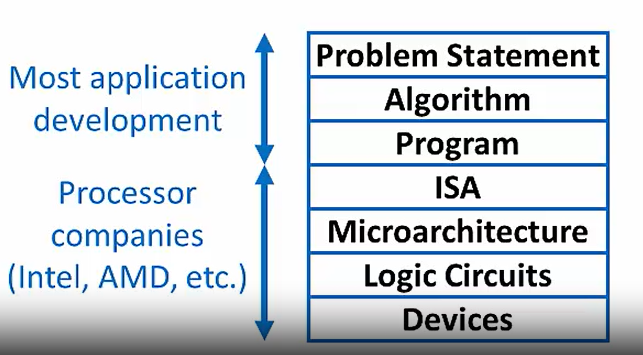
越在上层越抽象 more higher layer more abstraction
Problem Statement
natural language
ambiguous,imprecise
—— Software Design: Choose algorithms&data structures tosolve the problem
Algorithm
step-by-step procedure,guaranteed to finishi
Definiteness, effective computability, finiteness
—– Programming: Use a programming language to implement design
Program
Express the algorithm using a computer language
High-level language, low-level language
区分不同level看hardware还是software
low-level language: assembler, based on ISA
high-level language: complier, based on PS
—– Compilation: Use a compiler to convert the program to machine instructions
ISA
Specifies the set of instructions the computer can perform
Data types, addressing modes
—– Processor Design: Choose high-level organization and structures to implement ISA
Microarchitecture
Detailed organization of a processor implementation
Different implementations of a single ISA
—– Logic/Circuit Design: Choose gates and other low-level structures to implement components
Logic Circuits
Combine basic operations to realize microarchitecture
Many different ways to implement a single function(e.g., addition)
—– Implement & Fabricate: Transform logic circuits into masks for transistors and other layers, then fabricate
Devices
Transistor-based implementation of logic circuits
Chip layout masks
Properties of materials, manufacturability
Abstraction to Manage Complexity
higher level of abstraction = more abstract
Electrical Information
Almost all computing systems are digital
Analog:Continuous range of values
Digital:Discrete set of values (more abstract)
Digital is an Abstraction of Analog
Binary Information
Any data processed by a digital computer is represented by sequences of 1s and Os
Week02
Positional Notation
Digits represent powers of the base(radix)
Each digit D in radix r is restricted to $0≤D< r$
N-digit non-negative integer with radix r:
$D_{N-1}….D_1D_0= D_{N-1}×r^{N-1} + …+ D_1×r^1 + D_0×r^0$
Binary (Base 2) Octal (Base 8) Hexadecimal (Base 16)
Each position represents a power of base
Digit value says how many of that power of base
Value vs. Number
A value is a particular quantity
A number is a way to represent a value
To know the value indicated by a number, you need to know the format!
The contribution of each digit to a number’s value is determined by its position and the base
Conversion
Decimal to others: divide by base, the remainders are the digits
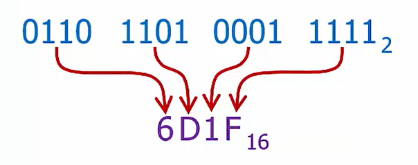
Binary to Hex: Directly substitute a hex digit fora 4-bit binary number (or vice versa!)
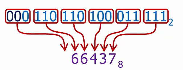
Binary to Octal: Directly substitute a hex digit fora 3-bit binary number (or vice versa!)
Octal to Hex:
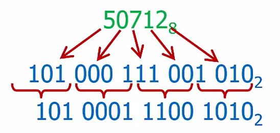
Use binary as an intermediate form!
Decimal to Octal, Decimal to Hex: use Binary as an intermediate form
left: most significant, right: less significant
Multiply: move to left, Multiplying a base $R$ number by $R^N$ “shifts” the number left by $N$ positions
Divide: move to right, Dividing a base $R$ number by $R^N$ “shifts” the number right by $N$ positions
Signed Number
In decimal, we show a number’s sign using asymbol (+ or -) in front of its magnitude Hence the name “signed-magnitude”…
2’s-Complement Representation
Positive numbers start with 0
The rest of the bits work the same as unsigned binary
Negative numbers start with 1
The interpretation is more complex
十进制负数 到 二补数:-5 到 5 -> 0101 -> 1010 + 1 = 1011
二补数负数 到 十进制负数1101 -> 0010 + 1= 0011 -> 3 -> -3
Addition
Addition works the way it does for unsigned binary numbers
Subtraction
Instead of subtraction with borrowing, we add the negation of the value we wish to subtract
This method simplifies computer hardware
Operand/Result Bitwidths Match
Operands and results must have the same number of bits for the math to work correctly
operand是符号两边的数字
Signed Extension
前面是0就补0,是1就补1
每种表达的范围,超出范围就overflow
unsigned number: $[0,2^{n}-1]$
signed number: $ [-(2^{n-1}-1),2^{n-1}-1 ]$
2’s-complement number: $[-2^{n-1},2^{n-1}-1]$
最小的数为1+n-1个0,最大是0+n-1个1,$[1000,0111]$
Overflow
不管哪种方式,只要大于以上表达数的范围就overflow,表现为显示答案错误,sign错误
The result cannot be correctly represented in the required number of bits.
lf adding two negative 2’s-complement numbers overflows, the sign of the result will appear to be non-negative.
1101 -3 |1001 -7
1100 -4 |1100 -4
————————
1001 -7 |0101 5 overflow
lf the result of adding two positive 2’s-complement numbers appears to be positive, then the operation did not overflow.
lf adding two unsigned numbers overflows , the result will appear to be
smaller than it should be.
Week03
Fixed Floating
When the format defines a “fixed” position for the radix point within the number’s digits, it is called fixed-point
Floating-Point
Floating-point: the format defines a way to encode the radix point location into the number(i.e., the position is not “fixed” in one place)
More flexibility than fixed-point… and more complexity!
Scientific Notation is floating-point
IEEE 32-Bit Floating-Point
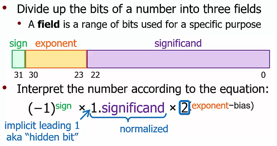
$(-1)^{sign} 1.signficand 2 ^{exponent-127}$
Format Comparison
Range: from the leftmost to the rightmostrepresentable values on the number line
Precision: number of significant digits
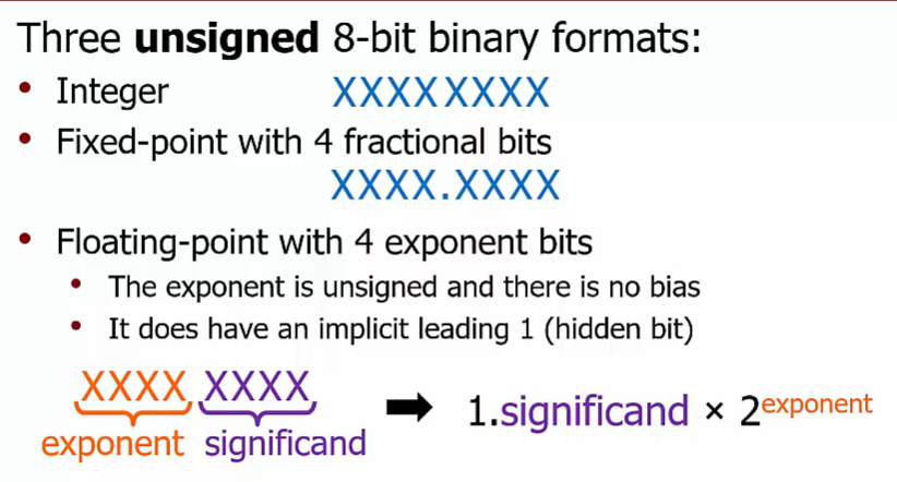
Integer: $XXXX XXXX$
precision: 8 bits
range: $[0,2^8-1]$
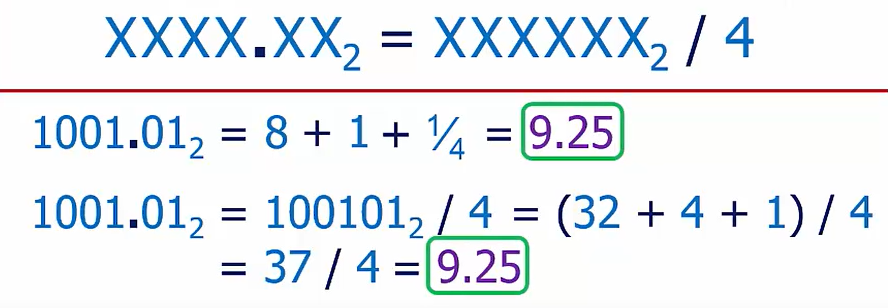
Fixed: $XXXX.XXXX$
precision: 8 bits
range: $[0,2^4-1+ 1- 2^{-4}]$
Float: $1.XXXX * 2^{XXXX}$
precision: 5 bits notes(不需要转成十进制) precision=1+significand
range: $[1,(1+1-2^{-4} )* 2^{2^4-1}]$
A 32-bit IEEE floating-point number has greater range and lesser precision compared to a 32-bit 2’s-complement integer.
ASCII
A computer stores text in memory as binary
It uses 8 binary-bits, 2 hex-bits (has been extended) to represent 128 different characters
Alphanumeric characters A-Z, a-z,0-9, encoded to allow easy sorting and transformation
Week04
Logic Functions
Ones and Zeros
Digital circuits manipulate voltage levels that weconsider more abstractly to be ones and zeros
We call these circuits logic circuits because they operate on and produce Boolean results
Boolean variables have only two possible values
TRUE (corresponding to “one”)
FALSE (corresponding to “zero”)
Logic Operator
AND: $A \cdot B$
OR: $A + B$
NOT: $\bar{A}$
XOR: $A \oplus B$ 相同是0,不同是1
The Odd Function
ex:$(A \oplus B) \oplus C$
output is 1 only when an odd # of the inputs are 1
Bitwise Logic Functions
A bitwise operation computes each bit of an N-bit result based on the value(s) in the
corresponding position of the N-bit operand(s) 按位运算
Combinational Logic
we think of logic circuits as having Boolean input values and producing Boolean results
In reality, they are built from transistors that connecteach output to power or ground based on the design of the circuit and the voltage level of each input
Logic circuits are at a higher level of abstraction
Each transistor acts like a switch…
Transistors
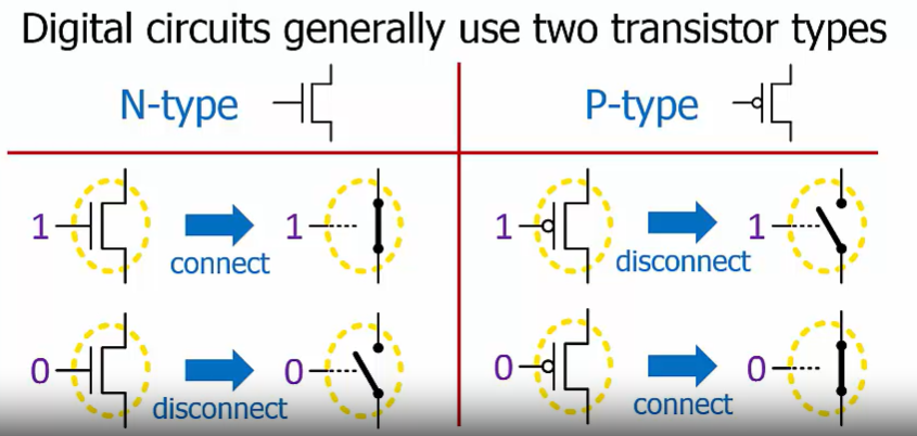
A logic gate is an electric circuit that contains transistors that connect the output to power or ground based on the input voltage(s)
power -> voltage interpreted as logic 1
ground -> voltage interpreted as loaic 0
NOT gate use 2 transistors
Logic Gates
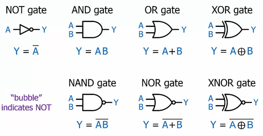
The shape of the gate allows us to visually determine all of these.
The inputs of these gates don’t need to be labeled because in these functions, the order of inputs doesn’t matter.
Combinational Blocks
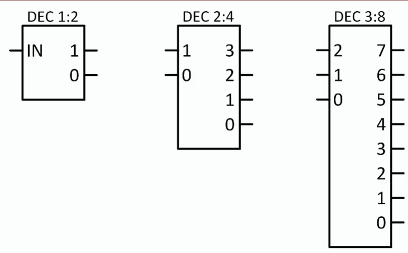
Decoder
Converts an n-bit input codeword into a unique m-bit output value, where $m=2^n$
Exactly one output can be true at any given time
Here we are only concerned with how the decoder behaves, not how it is constructed internally
If the input value is N, the output is N
When we represent a logic structure with a block, the internal details are hidden. When using the block in a logic circuit, we only need to know what the block does.
Inside the block’s symbol, we label each pin to indicate the pin’s function in the underlying logic structure.
When we draw signal names or Boolean values on the outside of the block near the pins, they indicate what is externally connected to the block (the Boolean value or signal name.
We label each decoder output with a decimal number that is equal to the input code value that causes that output to be 1.
A decoder indicates what number is present at the decoder’s input(s) by making the decoder output pin labeled with the same number output the value 1.
Multiplexers(Muxes)
Selection: based on the select input(s), choose one of the data inputs to drive the output
Output is equal to one of the data inputs
Select inputs indicate which data input
n select lines, $2^n$ input lines
The output of a multiplexer always has the same value as one of its data inputs.
The multiplexer’s select inputs control which of its data inputs is sent to the output.
A multiplexer chooses between multiple signals by outputting the data inputlabeled with the same number as current value of select input(s).
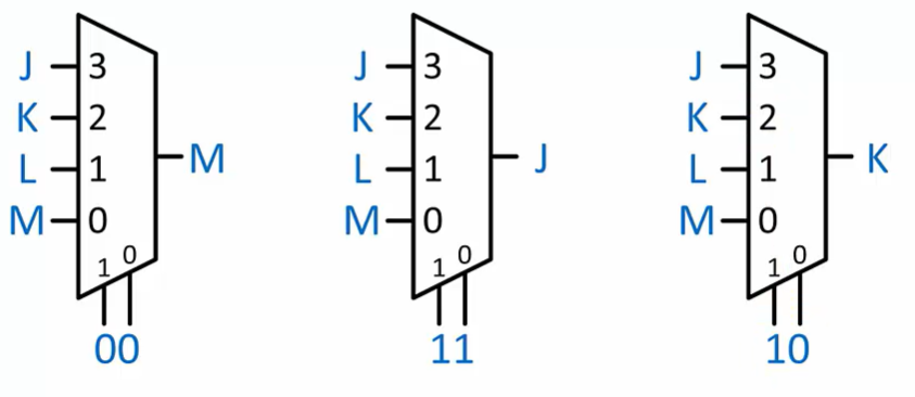
Data inputs must be labeled to indicate which input is chosen for a given select value
Select inputs must be labeled so we know the ordering of bits within the select value We need to interpret the select as a binary number
Exception: a 2:1 mux has only one select signal so it does not need a label
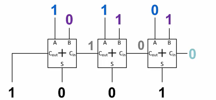
Adders
Full adder:
A structure that performs the addition for one bit position of a multi-bit binary addition operation.
Accept three inputs: a bit from each addend and a carry value from bit position to the right
Produce two outputs: the sum bit at that position, and a carry value to send to the bit position to the left
A full adder performs addition for a single bit position
Cout,Cin: 进位
Ripple Carry Adder
A series of full adders, where each full adder performs the addition for a single bit position.
Week05
Combinational Logic
So far, all of the logic circuits we have talked about have been combinational
Circuit outputs only depend on current input values
Adder, Mux, Decoder,
Sequential Circuits
The behavior of a sequential logic circuit is determined by both its current and past input values.
flip-flop, register, fsm
Some systems need to store information about past behavior to know how to react to inputs
Sometimes just need to store data for later access
Logic circuits whose outputs depend at least in part on past input behavior.
A circuit’s current state is the binary number that is currently stored in the circuit’s flip-flops.
The state of a sequential logic circuit can change, only at the triggering (active) edge of its clock signal.
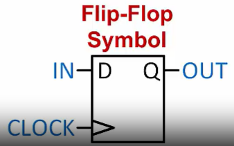
Flip-Flop
It has one bit of data input, one bit of data output
It also has a “clock” input that controls when the value carried by the input signal is stored into the flip-flop
The value held by a flip-flop cannot change until the clock allows it(or power is lost to the system…)
The flip-flop’s output is always equal to the value it is storing
Clock signal
A clock is a special signal that oscillates between 1and 0 at a specific frequency
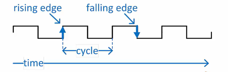
This D flip-flop updates when the clock transitions from 0 to 1(rising edge)
The flip-flop input is only stored at the rising clock edge(“triggering” edge)
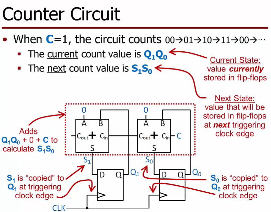
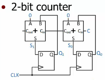
Counter Circuit
约等于每次给自己加1
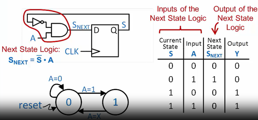
Finite State Machine
Any practical sequential circuit is a Finite State Machine (FSM)
State: current “status” -> the contents of the flip-flops
state diagram of a Flip-Flop only 2 state
counter state diagram only 4 state
Each state in an FSM is assigned a binary code
The FSM contains one flip-flop per bit of state
During operation, the code stored in the FSM’s flip-flops tells us (and the machine) which is the current state.
The next state becomes the current state when the flip-flop contents are updated
The FSM’s behavior depends both upon the current state and the input(s)
- The next state is a function of the current state and current input values
A state diagram describes the behavior of a state machine by showing for each state, what it should do in response to the inputs.
A given row of the state table lists the output value(s) it will produce for that row’s current state.
Hardware Design
A register is a group of flip-flops used to storemulti-bit binary values
Register Memory
Register
A register is a group of flip-flops used to store multi-bit binary values
Counter
Use adders and registers
Enable
Sometimes we want a flip-flop to “hold” its value for multiple clock cycles, regardless of its input
- But a flip-flop always stores the input value at the triggering edge of the clock…
Solution: add logic so that we can choose to store a new value or the value already in the flip-flop
- Selection based on the value of a special input signal called an enable
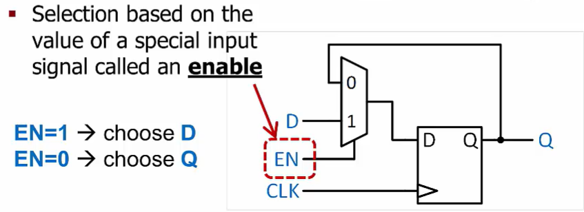
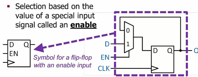
If we want to hold a value for longer, we can add a set of multiplexers full adders AND gates to choose between an external input value and the current register value.
The register’s clock enable signal selects which of those values will be stored into the register at the next triggering clock edge.
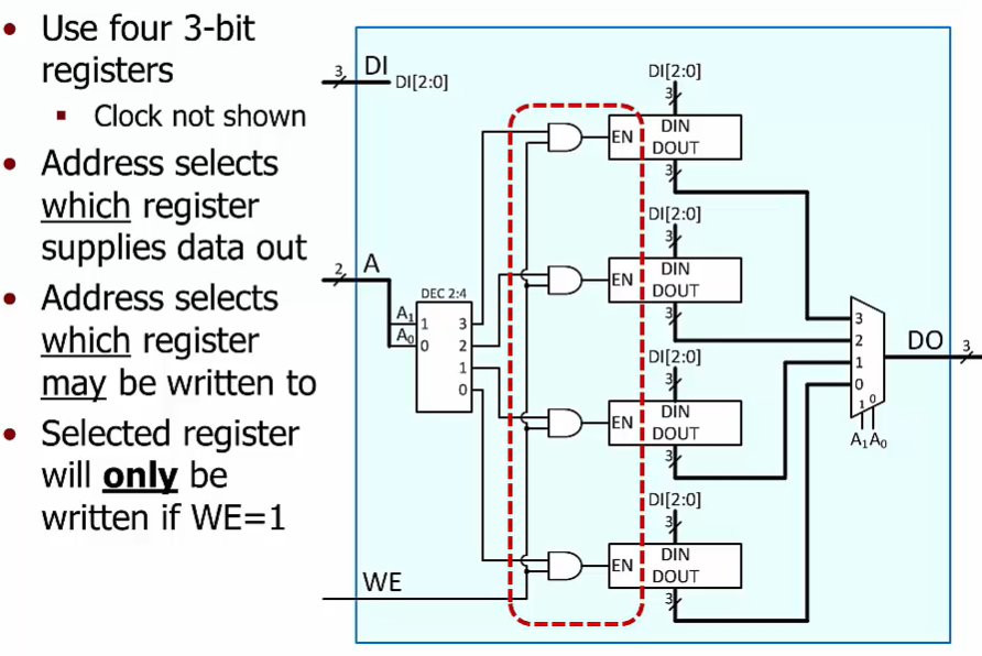
Memory
$M$-bits number specifies $2^M$ locations
Each location stores a single N-bit word
$N$ is the data size of the memory
The capacity of a memory is: $2^M * N$
A memory is conceptually like an array of registers
The capacity of a memory is equal to the total number of registers it contains.
Only one location can be accessed at a time,either to write (store) a value or read a value
To access a register, we index into the array using the address for that register
set WE to 1 for write, WE to 1 for read
In a memory :
$n$-bits address for $2^n$ locatioins
the number of address bits dictates the maximum number of addressable locations in the memory
Address selects which register supplies data out using muxs
Address selects which register using decoders
The data word size (# bits per data word) of a memory dictates 1.The number of data input and data output pins that the memory must have. 2. The number of single-bit storage elements required per memory location.
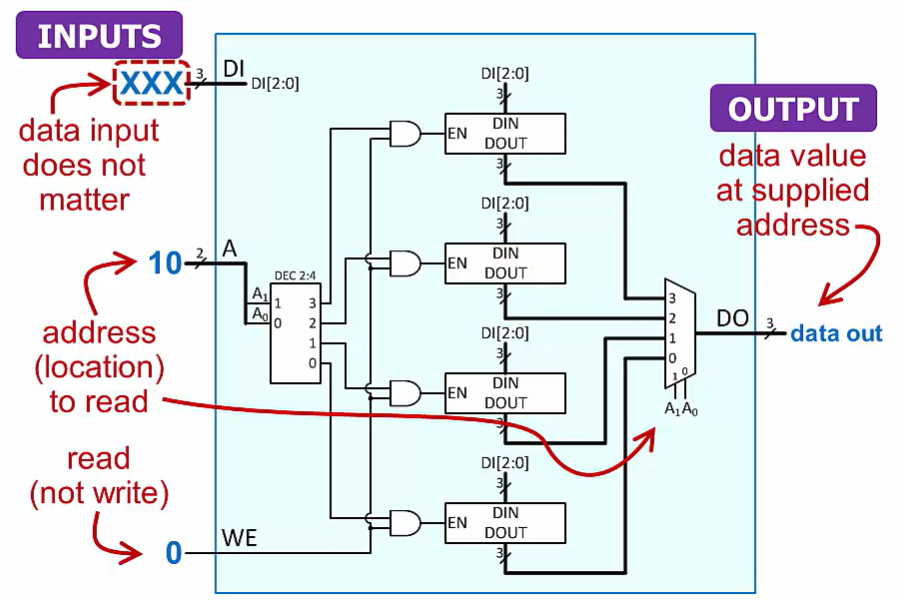
Read
using mux to select output location from read
no inputs and we
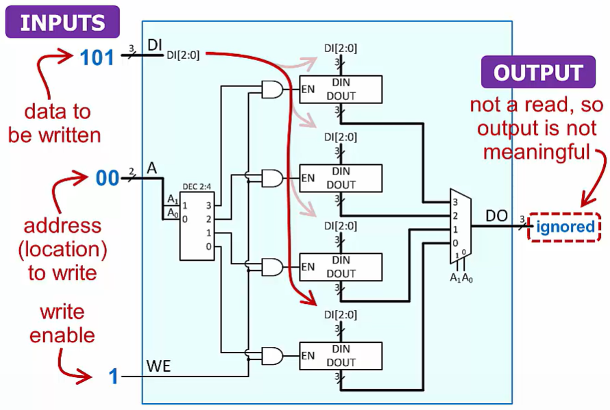
Write
input data, using decoder to select address to write, we enable
no mux and output
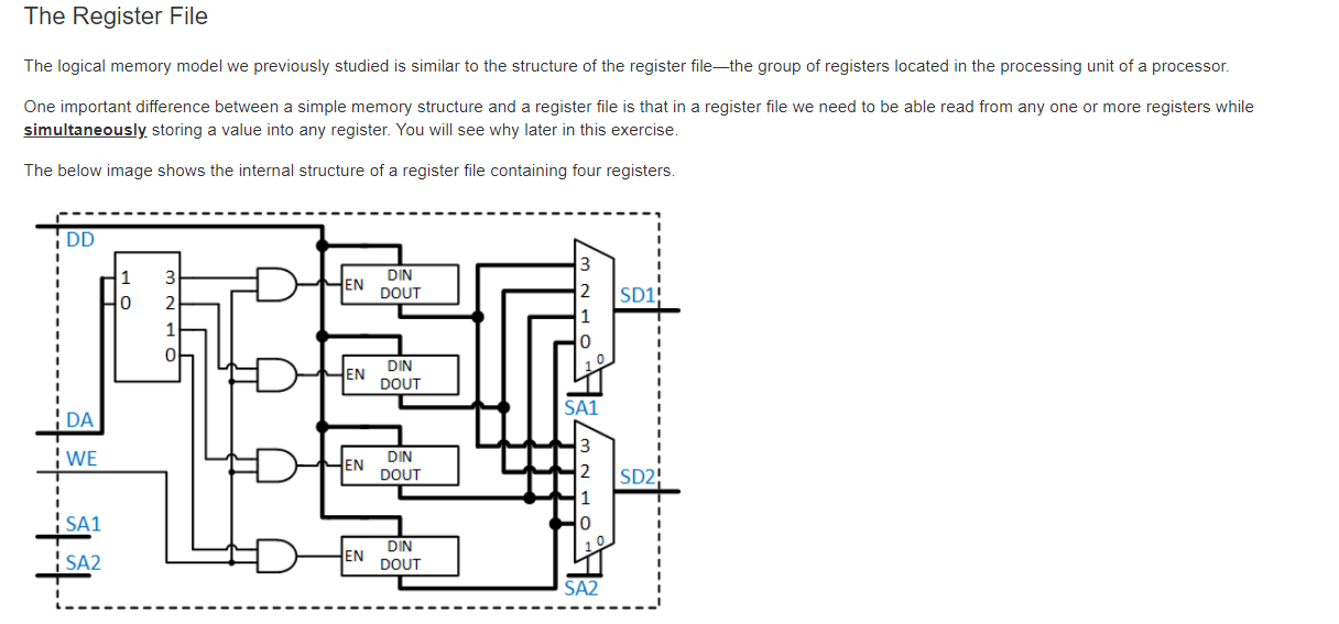
读进去mux SD1 SA1 SD2 SA2,对应的 bit也是对应
写入DA 地址,DD data 进入decoder
Week06
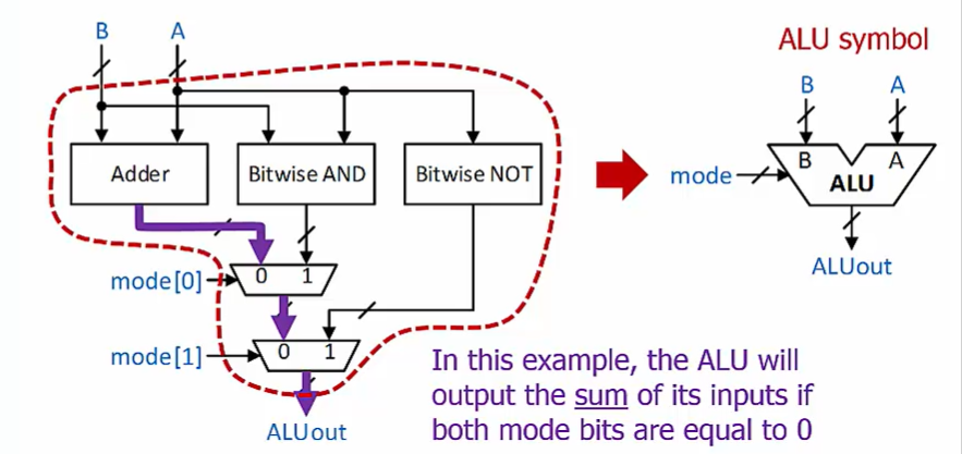
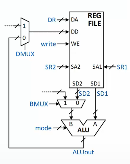
ALU(The Arithmetic Logic Unit)
A set of logic structures that perform a set of different possible computations on the inputs.
One or more arithmetic operations (e.g., add, subtract).
One or more logic operations (e.g.,AND,OR,NOT)
Includes a set of multiplexers that, based on a set of control signals, choose which result to send to the ALU output
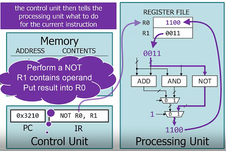
The Register File
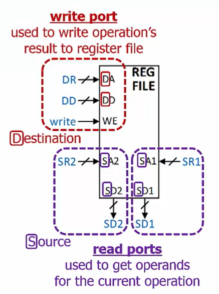
DA data address, DD data
A register file is asmall memory located near the ALU
Read from multiple locations and write toone location
Address inputs control which registers are accessed
Write enable controls whether the destinationinput is stored or not
In the register file, the decoder structure chooses which register is written to, and the multiplexer structures choose which registers are read from.
The Processing Unit
Contains the ALU and the register file
Control signals dictate which operation is performed on which data and where the result is stored
A program is a sequence of instructions, each of which describes one “step” of the program
One computer processes one instruction at a time
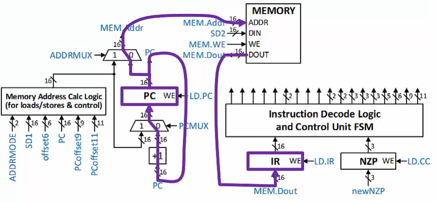
Control Unit
Fetches instructions one by one from memory
Tells each part of the computer what to do to execute each instruction
It tells the processing unit and the memory what to do in response to each instruction
It keeps track of which instruction in the program should be fetched next
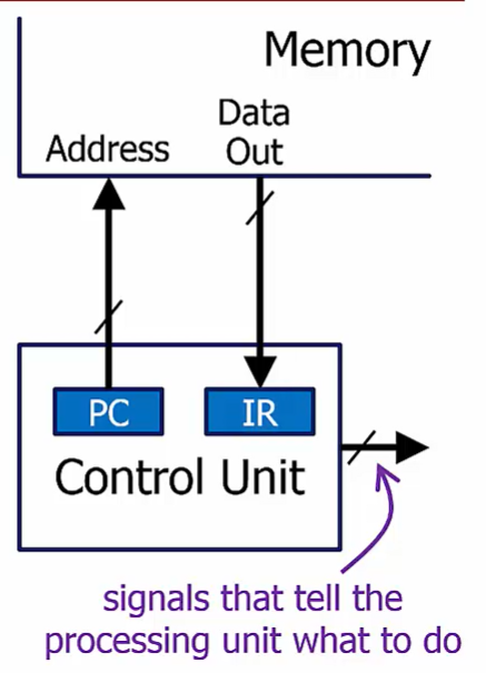
Contains two specialregisters:
Program Counter (PC): contains the address of the next instruction
Instruction Register (IR): contains the current instruction
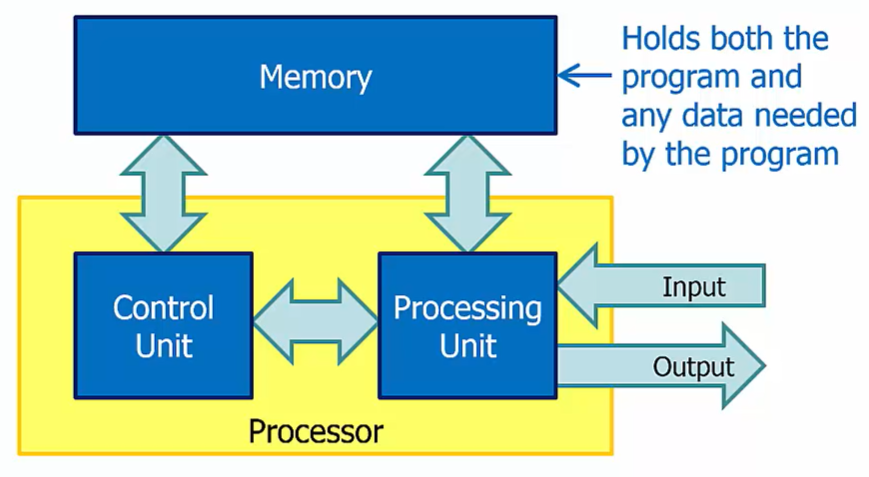
von Neumann Compute Model
In the von Neumann compute model, instructions and data are stored in memory
Another key feature of the von Neumann model is the fact that instructions are executed one at a time
In a computer, an instruction consists of two parts, the opcode, which specifies what the instruction does, and the operand(s), which specify the data it operates on.
Instructions are encoded as binary values and stored in the computer’s memory
Instructions
Instructions are divided up into fields (groups ofbits), each providing into about the instruction.
A program is a sequence of instructions
The fields and their sizes are also dictated by the ISA
Opcode: indicates the operation type (ADD, JMP, etc).
Other bits indicate operands and other information
Instructions from other ISAs will look different· Different number of bits, different fields, etc.
In a stored-program computer, the instructions that make up a program are stored in memory. This means that
By storing different sequences of instructions in memory, we can make the computer do different things.
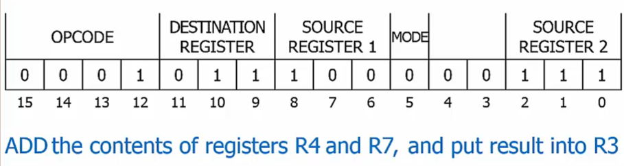
Five fields: opcode, destination register, source register 1, mode, source register 2
Each field represents a separate piece of information about the instruction
Operate Instructions
Use the ALU to perform a computation
Operands include value(s) in register file and possibly a constant encoded in the instruction
ex : R3 <- R4 +R7
R0 <- R0 +1
Data Movement Instructions
Copy data between the memory and register file
Allows processing of more data than can fit in theregister file (which is often relatively small)
Load - copy from memory to the register file
Store - copy from the register file to memory
ex: R1 <- mem[R5 + 2] : read from memory using an address 2 greater than contents of R5,and put the result into R1
Control Instructions
Change the sequence of execution by changing the value in the Program Counter (PC)
Loops: need to execute instructions more than once
If/else conditions: need to skip certain instructions.
Subroutines (similar to functions or methods in C/Java)
ex : PC <- R6 : overwrite the PC with the value in register R6
Instructions Cycle
Describe the different phases of execution of each instruction
Not all phases required for every type of instruction
Repeat forever
The control unit performs different tasksin each phase
It is a fsm
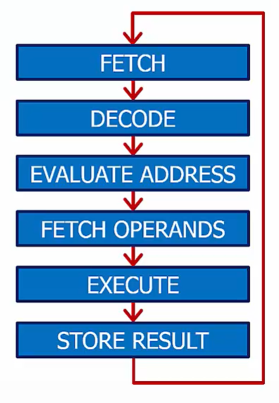
Fetch: The next instruction is read from memory
Decode: The control unit determines what the components of the processor should do based on the value in the instruction register (IR)
Evaluate Address: If a memory operation is needed, the address for it is calculated
Fetch Operands: One or more operands that are needed for an operation described by the instruction are read from memory or from the register file
Execute: Performs the “work” described by the instruction
Store Result: The result of the operation is written to the destination register indicated by the instruction
Fetch
- Read an instruction from memory
Address of the instruction contained in the PC
- Put value read from memory into the IR
The binary value that represents the instruction
- Increment the PC to”point” to the next instruction in memory(the next memory address)
Decode
Determine what the instruction says the processor should do
The instruction type is indicated by the opcode
Identify operands for the instruction based on the bit values in the
instruction’s fields
FETCH and DECODE are needed for all
Operate
fetch operands, execute, store result
Get the operands
Read from register file using source reg. address(es) encoded in the instruction
If instruction uses a constant, extract its value from the instruction
Perform the ALU operation
Write to the register file.
Use destination reg. address encoded in instruction
Use data produced by ALU
Data Move (Load)
evaluate address, fetch operands, store result
Calculate the memory address that will be used to read from memory.
- May involve register read and/or extracting a constan
Read from memory
- Use address calculated in EVALUATE ADDRESS phase
Write to the register file.
Use destination reg. address encoded in the instruction
Use data value returnedfrom memory
Data Move (Store)
evaluate address, fetch operands, execute
Calculate the memory address that will be used to write to memory
- May involve register read and/or extracting a constant
Read from the register file.
- Use source register address encoded in the instruction
Write to memory
Use address calculated in EVALUATE ADDRESS phase.
Use data value that was read from the register file
Control
evaluate address, execute
Calculate the memory address that will be written to the PC
This is the address of the next instruction that will be executed
May involve register readand/or extracting a constant
Determine if the PC shouldbe updated (if conditionalbranch), and if so do it.
- Update if the condition is met or is unconditional jump
Week07
LC-3 Overview
Instructions are 16 bits wide, divided into several fields of information
Bits 15 through 12 are the 4-bit opcode
The opcode for the current instruction is in IR[15:12]
Remaining bits are divided up into various other fields(the exact set of fields depends in part on the opcode)
Processing Unit
Eight general-purpose registers in the register file
Referenced using a 3-bit register address
LC-3 assembly language:
R3 is register w/address 011
Data word size is 16 bits
Constant (immediate) values encoded into instructions are 2’s-complement format
- sign-extended to 16 bits before processing
Control Unit
Control Unit coordinates and controls processor resources to execute a program
Fetch
Read from memory using PC as address
Place value read from memory (the next instruction that will be executed) into the IR
Increment the PC
Control Signal
Finite State Machine and instruction decode logic generates signals to control other resources
Affected by the binary instruction in the IR
If current instruction is a conditional Control instructional output is also affected by condition codes (CCS)
- Change the PC only if the condition(s) indicated in the current instruction is/are true
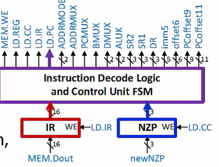
Condition codes (CCs) are stored in a special register
Indicate information about the most recent result in the Processing Unit
Negative, Zero, or Positive
Three 1-bit flags; exactly one of these equals 1 at any time!
Control Unit causes CCs to update as part of executing some instruction types
Operate instructions
Load instructions
Memory Address Calculation
Other logic calculates memory addresses.
Addresses used for Data Movement (loads/stores)
New PC value for Control instructions
- Remember - the PC holds a memory address….
- These calculations are specified by the ISA
The address calculation method depends on the memory addressing mode of the instruction
Add an offset to a value from the register file
Add one of two possible offsets to the PC
Offset values are decoded from the instruction
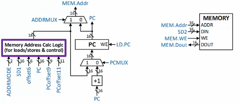
Memory
Holds both instructions and program data
- Memory’s DOUT (data out) output goes to both the IR in the Control Unit and to the Processing Unit
Only Data Movement store instructions write to memory
Memory’s DIN(data in) input comes from the Register File
16-bit memory addresses(range: 0x0000-0xFFFF)
16-bit memory data word size
- Same as size of instruction and register data word size
Operate Instruction
Perform computations using the Processing Unit
At least one source operand is read from the register file
May have $2^{nd}$ operand
Another register value
A constant encoded into the instruction itself
Performs an ALU operation
Writes the result back to the destination register in the register file
Sets/clears condition codes based on the result
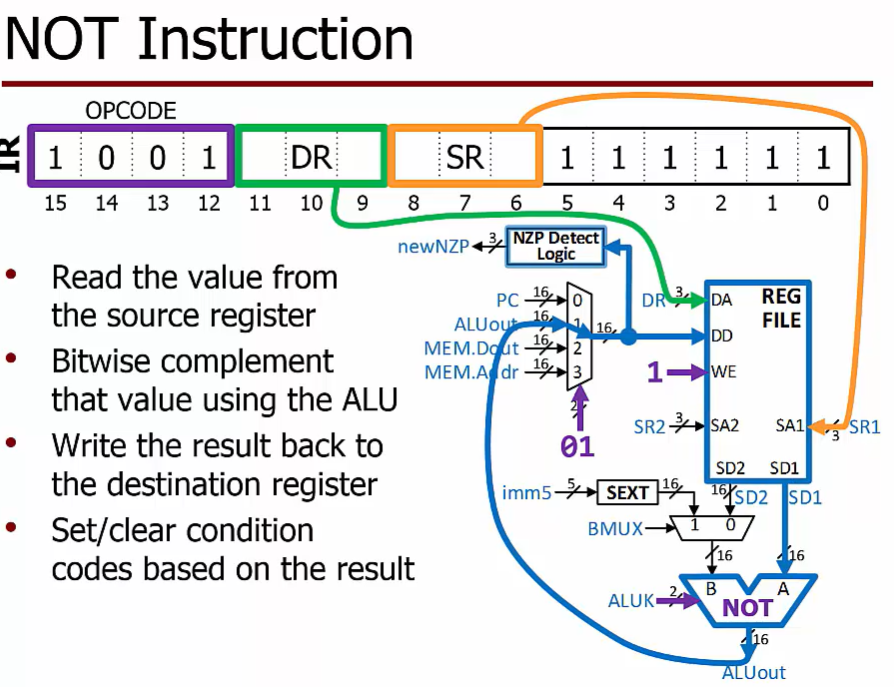
NOT
R register A address D data
D写入目标 S输入
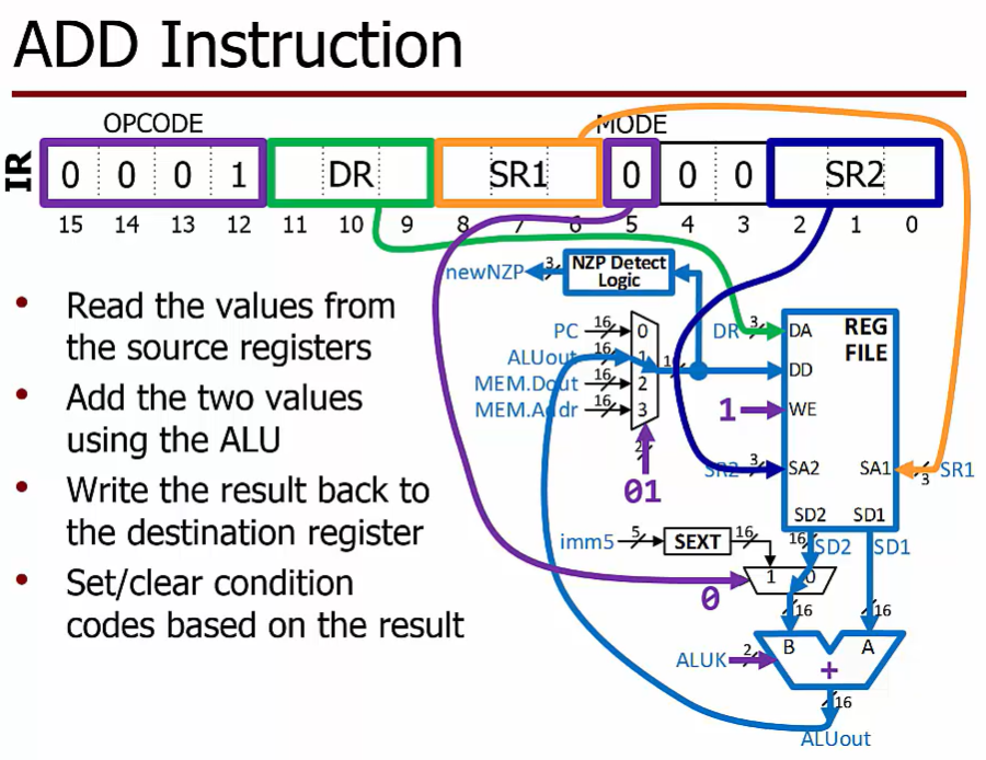
ADD
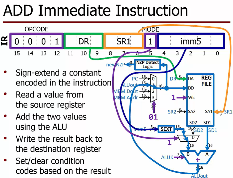
ADD Immediate
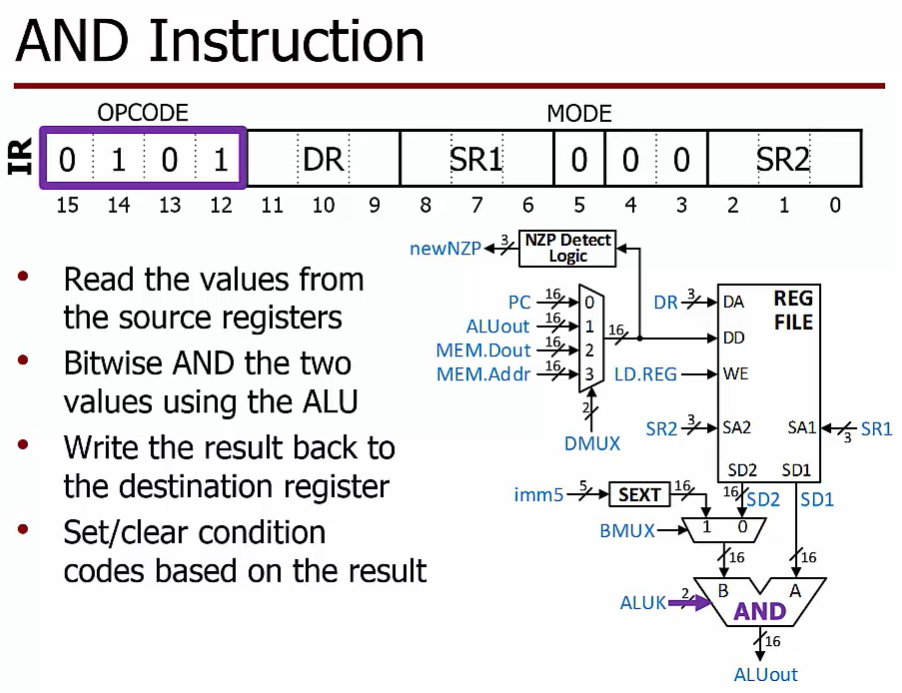
AND
AND Immediate
The 5-bit imm5 value (which comes from IR[4:0]) is sign-extended before being sent to the ALU.
How does the value of the SEXT logic’s output relate to the value of its input?
The output value is equal to the input value, but expressed with a different number of bits.
Simple Assembly Programming
Most people do not want to program in binary machine language…
Assembly language is close to machine language (still specify each instruction), but it has several features that make it easier to use
- Opcode mnemonics, comments, labels, symbols, etc…
The assembler translates assembly language programs into machine language that can be executed by the processor
- Performs low-level computations for the programmer.
- Creates an object file containing binary program instructions and other information
.ORIG started memory address
.END end of program
Initialization
赋值$R1$为$x$,Only works for values in range [-16,15] because the immediate is a sign-extended 5-bit number (imm5)
AND R1, R1, #X
Register Copy
ADD R1, R2, #0 ;R1 <- r2 and r1, r2, #-1 ; 0xffff Increment or Decrement
The ‘#’ symbol indicates that the number is given in decimal; ‘x’ indicates hex, ‘b’ indicates binary. Can represent 1210 as #12, xC, or b1100
If you want to use the minus sign, use decimal
ADD R7, R7, #1 ; R7=R7+1
ADD R6, R6, #-1 ; R6=R6-1
Negation and Subtraction
NOT R6, R6
ADD R6, R6, #1  ;negate R6

NOT R0, R4
ADD R0, R0, #1 R0 <- -r4 add r0, r3 ; r0 <- r3-r4
Masking
determine if a number is odd or even
AND R5, R5, #1 ; 1 means odd, 0 means even
# R2 <- 1 2*r0-r1 add r0, r0 not r1, r1 r2, Week08
Basic Data Movement
Similar to a variable in high-level languages
Assembler directives reserve space in memory and give them names that we can use to refer to addresses in our assembly-language program.
- The assembler converts these labels to the addresses the processor needs (…actually, a way to calculate them…)
The purpose of a load instruction is to copy a data word from memory to the register file. From the processor’s point of view, it loads a value from memory.
To execute a load or store instruction, the processor must calculate the memory address of the location to be accessed, which is called the effective address.
The method by which the address is calculated for a specific instruction is referred to as the addressing mode.
LD function
A load instruction copies a value from a memory location to a registerLD R0,NUM
copy whatever is in the memory location named NUM to register R0
LD DR, label ; Load from mem(PC-relative)
$DR <- mem[PC^+ + SEXT(PCoffset9)], setcc()$
ST function
A store instruction copies a value from a register to a memory locationST R6,NUM
copy whatever is in register R6 to the memory location named NUM
ST SR, label ; Store to men(PC-relative)
$mem[PC^+ + SEXT(PCoffset9)] <- SR$
Idea: instead of encoding the actual address, encode how far away it is from where the Program Counter is pointing
- This is called a PC-Relative addressing mode
$PC^+$ used here to mean “already-incremented PC”
These instructions are used for accessing memory “near” the current PC value
- 9-bit 2’s-complement offset means the address must be within [-256,+255] of the already-incremented PC
More Data Movement
LDR and STR use Base+Offset addressing.
The base register acts as a “pointer”into memory.
The signed offset indicates how far away the effective address is from where the base register is pointing
LDR function
LDR R5, R1, #2
read whatever is in memory two steps past the address in R1, and copy it to register R5
LDR DR, BaseR, offset6 ; Load from men (base+offset)
$DR <- mem[BaseR + SEXT(offset6)], setcc()$
STR function
SRT R5, R1, #2
copy whatever is in register R5 to memory two steps past the address in R1
STR ST, BaseR, offset6 ; Store to men (base+offset)
$men[BaseR + SEXT(offset)] <- SR$
LEA function
LDR and STR are only useful if we first put a useful address into a register!
LEA copies a label’s address to a register
“Load Effective Address”
- The effective address for LEA is calculated exactly the same way as it is for LD and ST (PC-Relative)
LEA DE, label ; Put label address into reg
$DR <- PC^+ + SEXT(PCoffset9), setcc()$
LEA R1, ARRAY
Memory Indirect
LD and ST allow us to access labelled memorylocations “near” the instructions
- The distance is limited by the size of the PC offset field
LDR and STR are more flexible…
Can access locations around a “nearby” label.
- Use LEA to get a label address into the base register
- Then use LDR/STR to access locations at/near base address
Can access any address
  - Use a .FILL directive to create a location holding an address
  - Use LD to load the address from memory
Then use LDR/STR to access locations at/near base address
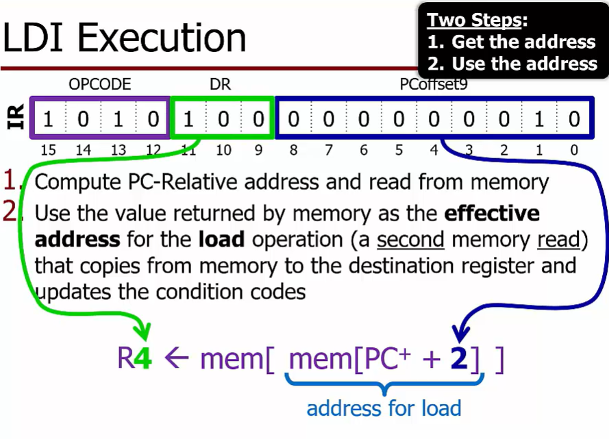
LDI function
read from the location labeled ADDR_R to get the effective address for a load that copies from memory to register R4
Load using Memory Indirect
LD R1, ADDR_R
LDR R4, R1, #0
LDI R4, ADDR_R
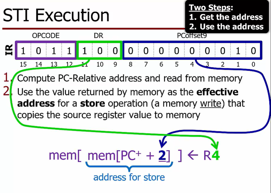
STI function
read from the location labeled ADDR_w to get the effective address for a store that copies from register R4 to memory
Store using Memory Indirect
LD R2, ADDR_W
STR R4, R2, #0
STI R4, ADDR_W
Week09
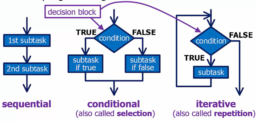
Flow Chart
Flowcharts graphically represent programs during their design
- Writing code for a flowchart is the easy part!
Systematic Decomposition
Break down complex problems into a set of easier-to-handle tasks
Replace each task with set of smaller tasks and condition tests until each step is easy
Changing the Flow
The next instruction to execute does not have to be in the next location in memory
Branch instructions allow the program to change the value in the PC
- Unconditional branch: always updates the PC.
- Conditional branch: only updates the PC(is taken) if some specified condition is true
- If the condition is false, the branch is not taken, and the next
instruction to execute will be the one at the memory location just after the conditional branch instruction - The new PC value is called the branch target
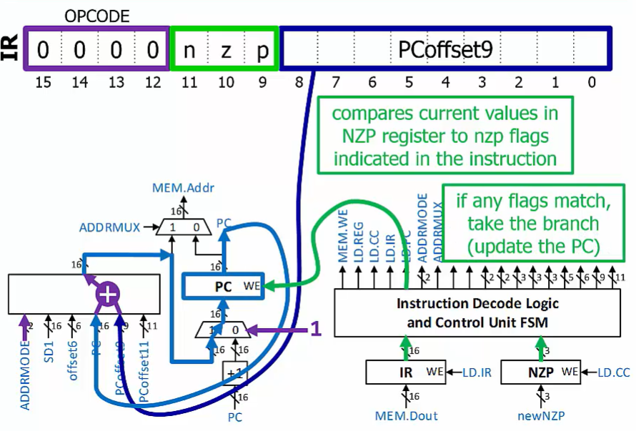
BR Instruction
Calculate the branch target by adding the sign-extended offset to the already-incremented PC
Compare conditions indicated in the instruction with the current NZP condition code values.
If any match, then update the PC with the calculated branch target
If none match, do not modify the PC
Note: even if the BR does not modify the PC, the PC was incremented when the BR was fetched
BRx label
; Conditional branch to label, x is condition
$PC <- PC^+ + SEXT(PCoffset9)$
值得注意的是PC是已经incremented的所以指向BR的下一行,offset也是从下一行开始算要加多少行
z =0, zp >= 0, np !=0, nzp= uncnditionally
看的时候只要NZP这三个框有一任意在指令里的是1就行,例如指令是zp,control是NZP 001 符合
JMP
The distance of a BRanch target is limited by the range of offsets encoded in the instruction
- 9-bit offset,range [-256,255] from incremented PC
- If target code is at an address further away in memory,need to use a different instruction…
JMP is an unconditional jump instruction that updates the PC with the value in a register
JMP BaseR ; Jump to address in register
$PC <- BaseR$
Read value from source register
Write the source register value to the PC
Masking
bit从0开始
检查第n位是0,倒着来最低位都是0,第n位是1,$2^{n}$,BRz
检查第n位是1,倒着来最低位都是0,第n位是1,$2^{n}$ ,BRp
检查后几位 011001, 写了n位就是n个1,$2^{n}-1$, ADD R0, R0, #(1-2^n) , BRz
Week10
Assembly Language
Low-level language
One-to-one correspondence between assembly language instructions and machine instructions
As in all languages, you have to use correct grammar!
Advantages over machine language
- Mnemonics instead of numeric opcodes: A short sequence of letters that has the same underlying meaning as a specific opcode value, but also hints at what the instruction does.
- Symbolic names instead of numeric addresses
- Encoding of instructions Offsets, immediate values
lables store in symbol table
.ORIG and .END is assembler directives
.BLKW .FILL .STRINGZ is memory allocation directives
Running a Program
Assemble the source code
- Produce a program image (code and initialized data)
Load the program into the memory
- A real processor includes special hardware to write the assembled program binary into memory
- In a simulator, the binary program file is read and copied into the simulator’s model of the memory
Execute the program
- Often want to go through a program one instruction ata time, or run to a certain instruction and pause
- Simulators and hardware debug tools both provide this capability
Debugging
Debuggers usually provide two types of single-step execution that you can use:
Step into: executes one instruction and then pauses
Step over: like step into, but if the instruction is a subroutine call, executes the entire subroutine( including any subroutines it calls) before pausing
Breakpoints are another important tool that let you run the program up to a certain instruction.
- You can then check the register and memory values when execution reaches that point, and if needed, single-step from there
Memory Allocation
Allocate: reserve space in memory
- No other variable or code will be placed there
Initialize: set the value in a memory location when program is loaded
- In other words, before the program executes
.FILL value
Allocates one word of memory, initialized to the indicated value when the program is loaded
- The value in that location may be changed later by executing a store instruction
- Optional label can be used to refer to that location
.BLKW count
Allocates count words of memory
BLKW = “BLocK of Words”
The allocated memory locations are not initialized.
They may happen to be 0… or they may not…
Allocates and initializes memory to hold a null-terminated character string
- One word per character, where each character is represented by its ASCII code
- Last location holds the value 0 to indicate end of string.
- This is the ‘z’ in STRINGZ
- Also called the “null terminator”
Total allocated words = number of characters plus 1
Week11
Subroutines
Subroutines are well-defined software modules that are written to perform a specific task
- Functions and methods in high-level languages are implemented using subroutines
To use a subroutine, a program calls the subroutine
- The processor executes the subroutine code
- When the subroutine code is finished, the processor returns to the next instruction after the one that called the subroutine
A program can call a subroutine multiple times. Subroutines can also call other subroutines
More abstract approach to programming by encapsulating lower-level tasks
- Code calling the subroutine does not need to know the details of how the subroutine code actually works
Write modular code to simplify testing and increase possibilities for software reuse
- Testing a small subroutine is much simpler than testing an entire program
JSR
R7 <- already-incremented PC
PC <- address of label
If a subroutine calls another subroutine (or otherwise modifies R7), it MUST save a copy of R7 to memory before calling the subroutine, and then restore R7 before its RET instruction
Parameter Passing
Many subroutines require information from the caller to perform their task, and may need to return one or more results to the caller
- Commonly called parameters
Parameters can be passed to and from the subroutine in a variety of ways
- In registers
- In specific memory locations.
- On the stack
- A special data structure implemented in most processors
Pass-By-Value: value store in the register
Pass-By-Reference: address store in the register
Caller-save & Callee-save
Caller-save: the caller code is responsible for saving/restoring any needed register values.
- Store the values in those registers to memory before calling the subroutine
- Re-load the saved values after the subroutine returns
在调用子函数之前存好register
Callee-save: the subroutine is responsible for saving/restoring any modified register values.
- Subroutine must appear to not modify registers.
- …..except for those used to hold results
- ….and the register that holds the return address (R7)!
Referred to as context save and restore
Disadvantage:
. The subroutine may unnecessarily save/restore registers that the caller is not using
Advantages:
. Only a single copy of the register save/restore code is present,regardless of how many times the subroutine is called
· Callers can freely use subroutines, knowing that the subroutine will not corrupt any registers
Callee-save is normally used (with one exception). A caller must save R7 before calling a subroutine,since that call will overwrite the value in R7
Week13
I/O concept
General-purpose I/O (GPIO) pins
The most basic form of output is a pin that the processor can set to 1 or 0 (voltage levels). Turn a light ON or OFF
The most basic form of input is a pin that the processor can be read to determine its voltage level (1 or 0)
- Check if a button is pressed or not
Analog-to-digital converter ( input device)
- Sample an analog signal and represent it as binary data
Digital-to-analog converter (output device)
- Convert digital (binary) data into an analog signal
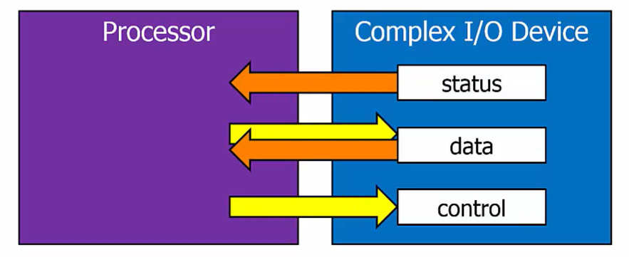
Complex I/O Devices
Most devices operate as both input and output
- Network interface
- Bluetooth radio
- USB interface
- Hard drive
I/O Synchronization
Processors run at a rate controlled by the clock
But, most I/O activity occurs at unpredictable times unrelated to the processor clock
- Example: Someone typing on a keyboard
This is asynchronous I/O
- Asynchronous means “not related to the clock”
For the processor to operate with asynchronous I/O devices, there must be a way for the processor to check if the device needs service
Unconditional / Conditional
Some simple I/O devices are always ready to accept or supply new data
For most I/O devices, we need to check if they are ready before transferring data
Isolated / Memory - Mapped I/O
Some processors use special instructions and a different address space to do this
- This is isolated I/O
Most processor use their normal load/store instructions to access I/O devices
To the processor, the I/O device registers appear to be normal memory locations… but they are not!
We set aside some locations in the memory space, and add logic so that loads/stores to these addresses access the I/O device registers instead of memory
Polled / Interrupt-Driven I/O
Polling is the process of repeatedly checking to see when something becomes ready
For example: we poll the keyboard to see if it has anew character; the answer is “no” until one is typed!
Processors also contain hardware that allows an I/O device to interrupt the processor
When I/O operations use interrupts, the I/O device announces to the processor (without the processor asking) that something has happened.
On the other hand, when I/O operations use polling, the processor repeatedly asks the I/O device if something has happened.
I/O Device Interface
Status registers: processor reads to check device state
- A keyboard sets a status register bit to indicate data is ready
Data registers: used for the exchange of data
- when a key is typed, a keyboard places the corresponding ASCII code in a data register for the processor to read
Control registers: processor writes to change how the I/O device operates
- A keyboard may have a backlight that the processor can turn off to save power when the computer is idle
- The processor may change the operating speed of a serial communications port
The data provided by a memory-mapped input device can be accessed by reading from the device’s memory-mapped Data Register
Data can be sent to a memory-mapped output device by writing to the device’s memory-mapped Data Register
LC-3 I/O
Keyboard Input
Registers:
Keyboard Status Register (KBSR) address = 0xFE00
- KBSR[15] is 1 if a new character is available, 0 otherwise.
- This use of KBSR[15] is a synchronization mechanism, and we refer to KBSR[15] as a flag that indicates if information is available.
Keyboard Data Register (KBDR) address = 0xFE02
- KBDR[7:0] contains the ASCII code of the last character typed
- Reading KBDR automatically resets bit 15 of the KBSR
Usage:
- To check if a character is available, read KBSR and test if bit 15 is 1. Is the value negative?
When a character is available, read it from KBDR
Read from KBSR, Get the value from KBDR, (address KBDR = KBSR + 2)
LD    R1, IO_BASE    ; start of memory-mapped I/O
WAIT            ; start of Poiling Loop
    LDR    R2, R1, #0
    BRzp    WAIT
    LDR    R0, R1, #2
Character Display Output
Registers:
Display Status Register (DSR) address = 0xFE04
- DSR[15] is 1 if the display is ready, 0 otherwise
Display Data Register (DDR) address = 0xFE06
- The character (ASCII code) written to the DDR will be displayed on the screen
Usage:
To check if the display is ready to accept a character,read DSR and check if bit 15 is 1
When the display is ready, write the character to DDR
LD    R1, IO_BASE ; start of memory-mapped I/O
WAIT
    LDR    R2, R1, #4    ; read from DSR +4
    BRzp    WAIT
    STR    R0, R1, #6    ; write to DDR +6
LDI/STI
The book uses LDI and STI for its examples; this video instead uses LD+LDR and LD+STR
- LDI is equivalent to LD followed by LDR
- STI is equivalent to LD followed by STR
Using LDI in a polling loop means two memory reads foreach iteration instead of one
- Remember - memory accesses are actually very slow…
- Why read memory repeatedly to get the status register address?
- We only read the IO_BASE address once, then use LDR/STR instructions with the appropriate offsets
Most modern processors do not have LDI/STI
- Performance issues outweigh any benefits
- Included because the idea of indirect access is important
OS
Allows applications to interact with I/o devices without having to have specific knowledge of all possible I/O devices
- Keyboard/mouse/pen/touchscreen input.
- Display/printer output
- Disk access
- Network access
All application-level I/0 is controlled by and goes through the os
- The system hardware usually prevents applications from accessing the I/O directly to ensure this
communicating with the OS: Need a mechanism that insulates the OS from the application (and vice-versa), but allows the
application and the OS to communicate
- Must be built into the processor itself so it cant be circumvented by malicious software
Processors provide an indirect mechanism for apps to request OS services
These are special instructions called software interrupts or traps
- Part of the instruction is a code used to identify the specific type of service requested
- Executing these instructions is a “system call”
These instructions transfer control to the operating system, which performs the service and then returns control to the application
LC-3 Operating System
How does the LC-3 processor access I/O devices?
- By interacting with memory-mapped I/O device registers.
A memory-mapped device register is a special register that is physically located somewhere outside of the memory and register file.
To use LC-3 OS services, you must assemble and load the LC-3 OS before loading your program
- Processor still starts execution at 0x0200, but now that location is part of the OS code
The OS jumps to 0x3000 to run your program, so your program needs to start there when using the OS
The TRAP instruction requests an OS service.
OS executes a service routine or TRAP handler
Returns to your program when finished
The LC-3 OS provides some basic I/O services.
- Reading from the keyboard
- Writing to the console display
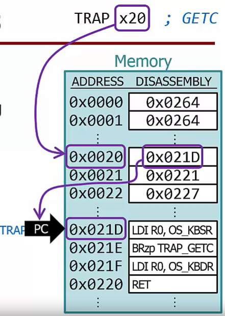
TRAP
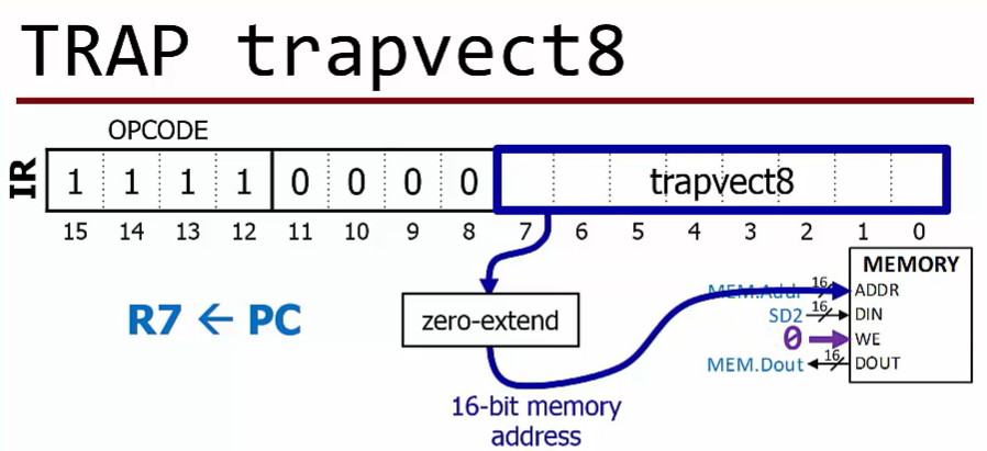
- Copy PC to R7
Zero-extend 8-bit code to use as address for reading from the vector table.
Addresses 0x0000-0x00FF
Value returned from table is written into PC
. The address of requested TRAP handling routineTRAP handlers return just like subroutines do
· All handlers end with RET
Uing TRAPS
Since TRAP uses R7 to hold the return address, code using R7 must save and restore it
There are six service routines, and the LC-3 assembler supports an alias for each
GETC TRAP x20 Waits for a character from the keyboard. ASCII code returned in R0[7:0]
OUT TRAP x21 Writes a character to the console display. ASCII code passed in R0[7:0]
PUTS TRAP x22 Writes an ASCIIz string to the console display. String address passed in R0
IN TRAP x23
Writes “Input a character>” to console display,then waits for a character from the keyboard.
ASCII code returned in RO[7:0]
Character is also echoed to the console displayPUTSP TRAP x24 not used in ECE 252
HALT TRAP x25 transfer control to OS and restart